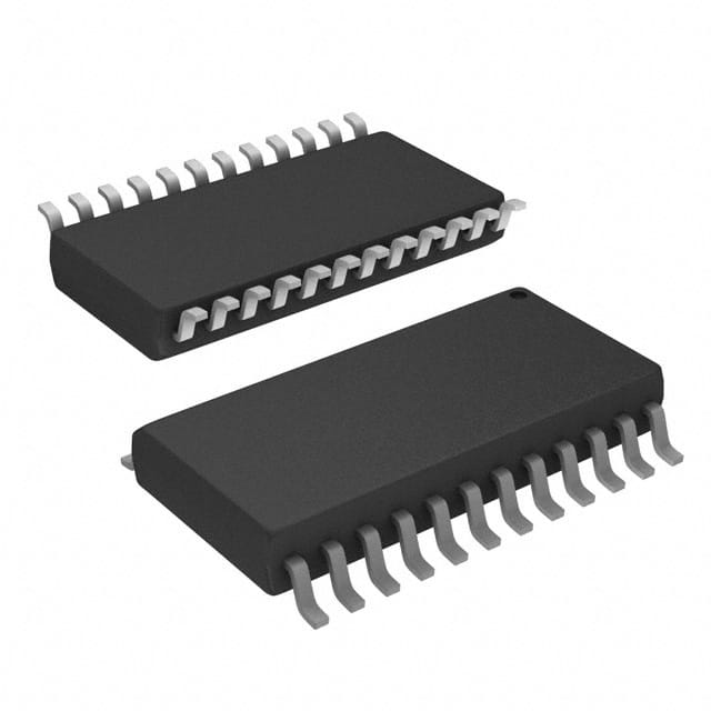
SN10KHT5541DW Texas Instruments IC OCT ECL-TTL XLATR 3-ST 24SOIC
Інтэгральныя схемы (ІС)
Нумар вытворцы:
SN10KHT5541DW
Вытворца:
Катэгорыя прадукцыі:
Апісанне:
IC OCT ECL-TTL XLATR 3-ST 24SOIC
Стан RoHs:
Табліцы дадзеных:
Асаблівасці :
-
Выхадны сігнал :
TTL
Каналы на ланцуг :
8
Колькасць контураў :
1
Напружанне - VCCA :
-
Напружанне - VCCB :
-
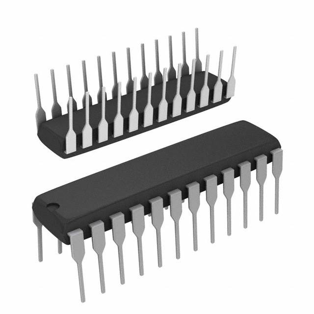
Пакет / Чахол :
24-SOIC (0.295", 7.50mm Width)
Пакет прылады пастаўшчыка :
24-SOIC
Працоўная тэмпература :
0°C ~ 75°C (TA)
серыял :
-
Тып вываду :
Tri-State, Non-Inverted
Тып канала :
Unidirectional
Тып мацавання :
Surface Mount
Тып перакладчыка :
Mixed Signal
Уваходны сігнал :
ECL
Ўпакоўка :
Tube
Частка Статус :
Active
Хуткасць перадачы дадзеных :
-
в наличии
50,870
Unit Price:
Звяжыцеся з намі Прапанова
SN10KHT5541DW Канкурэнтныя кошты
ChipIc мае унікальную крыніцу паставак. Мы можам прапанаваць SN10KHT5541DW больш
канкурэнтаздольную цану для нашых кліентаў. Вы можаце атрымаць асалоду ад нашым лепшым
сэрвісам, купіўшы ChipIc SN10KHT5541DW. Калі ласка, не саромейцеся звяртацца наконт
лепшай цаны на SN10KHT5541DW. Націсніце, каб атрымаць прапанову
SN10KHT5541DW Асаблівасці
SN10KHT5541DW is produced by Texas Instruments, belongs to Логіка - Перакладчыкі, Узроўнямеры.
SN10KHT5541DW Падрабязная інфармацыя аб прадукцыі
:
SN10KHT5541DW - гэта Логіка - Перакладчыкі, Узроўнямеры, буферныя ўзмацняльнікі, распрацаваныя і
вырабленыя
Texas Instruments.
SN10KHT5541DW вытворчасці Texas Instruments можна набыць на сайце Chipic.
Тут вы можаце знайсці розныя віды электронных дэталяў ад вядучых вытворцаў свету.
SN10KHT5541DW кампаніі Chipic прайшоў строгі кантроль якасці і адпавядае усім патрабаванням.
Статус запасаў, пазначаны на Chipic, прызначаны толькі для даведкі.
Калі вы не знайшлі запчастку, якую шукаеце, вы можаце звязацца з намі для атрымання дадатковай інфармацыі, такі як колькасць запасаў у табліцы дадзеных SN10KHT5541DW (PDF), кошт SN10KHT5541DW, Распіноўка SN10KHT5541DW, кіраўніцтва SN10KHT5541DW і рашэнне на замену SN10KHT5541DW.
SN10KHT5541DW FAQ
:
1. What is the maximum operating temperature for the SN10KHT5541DW?
The maximum operating temperature for the SN10KHT5541DW is 150°C.
2. What is the typical input voltage range for this semiconductor?
The typical input voltage range for the SN10KHT5541DW is 3V to 5.5V.
3. Can you provide the typical output current for this device?
The typical output current for the SN10KHT5541DW is 100mA.
4. What are the recommended storage conditions for this semiconductor?
It is recommended to store the SN10KHT5541DW in a dry and cool environment with a temperature range of -65°C to 150°C.
5. Does this semiconductor have built-in overcurrent protection?
Yes, the SN10KHT5541DW features built-in overcurrent protection to safeguard against excessive currents.
6. What is the typical quiescent current consumption of this device?
The typical quiescent current consumption of the SN10KHT5541DW is 50µA.
7. Can you explain the typical application circuit for this semiconductor?
The typical application circuit for the SN10KHT5541DW involves connecting the input voltage, ground, and load to the respective pins of the device, ensuring proper decoupling capacitors are used.
8. Is there a thermal shutdown feature in the SN10KHT5541DW?
Yes, the SN10KHT5541DW includes a thermal shutdown feature to prevent overheating.
9. What is the typical response time of this semiconductor in regulating output voltage?
The typical response time of the SN10KHT5541DW in regulating output voltage is 10µs.
10. Can you provide the package outline dimensions for the SN10KHT5541DW?
The package outline dimensions for the SN10KHT5541DW are 3mm x 3mm, with a height of 0.8mm.
SN10KHT5541DW Змяненні, ключавыя словы
:
SN10KHT5541DW Кошт
SN10KHT5541DW Малюнак
SN10KHT5541DW Напружанне на выснове
Акцыі: Хуткая праверка каціровак
Мінімальная замова: 1
Змяшчае прадукты серыі "SN10"