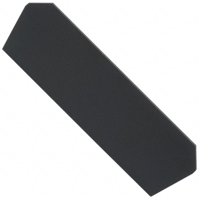
2003 Microsemi Corporation TRANS HBT RF BIPOLAR 55BT
Дыскрэтныя паўправадніковыя прыборы
Нумар вытворцы:
2003
Вытворца:
Катэгорыя прадукцыі:
Апісанне:
TRANS HBT RF BIPOLAR 55BT
Стан RoHs:
Табліцы дадзеных:
Выйгрыш :
8.5dB
Каэфіцыент узмацнення пастаяннага току (hFE) (мінімум) @ Ic, Vce :
10 @ 100mA, 5V
Каэфіцыент шуму (дБ Typ @ f) :
-
Магутнасць - Макс :
12W
Напружанне - прабой эмітэра калектара (макс.) :
50V
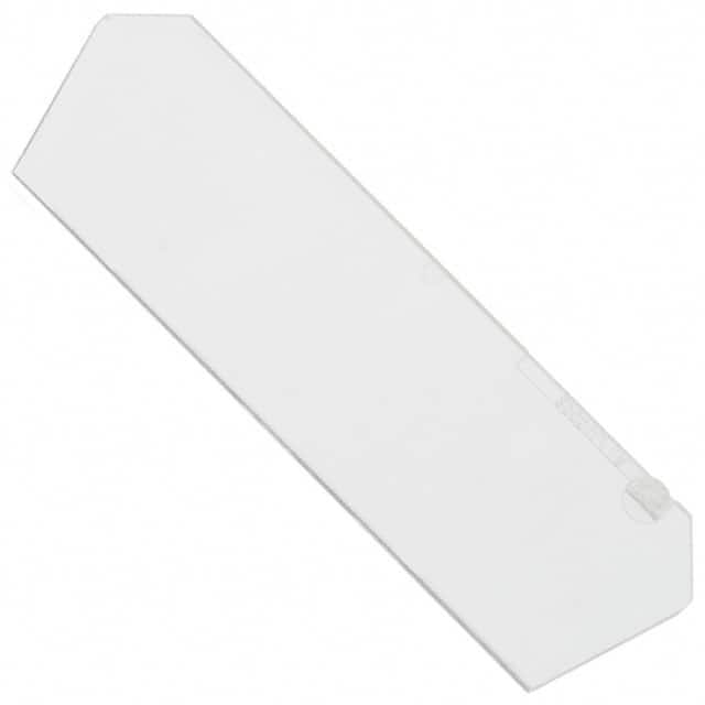
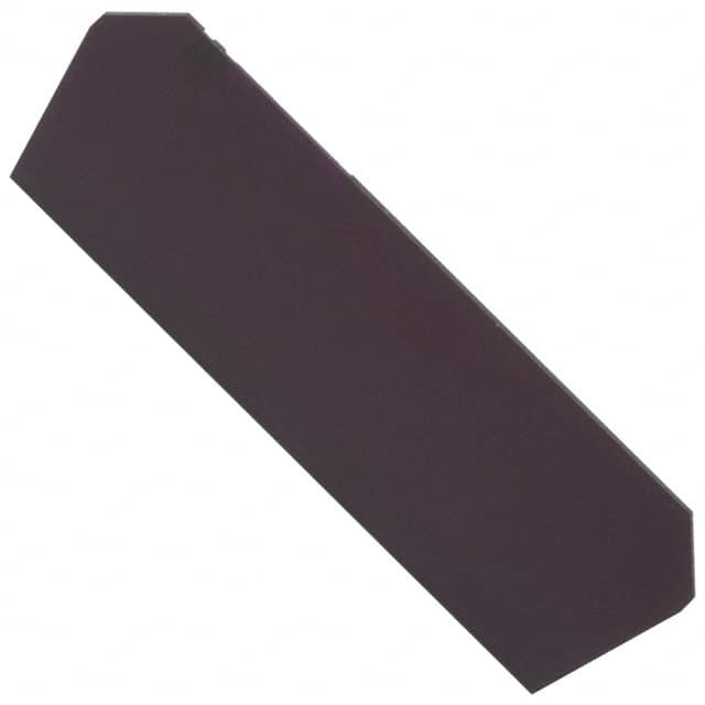
Пакет / Чахол :
55BT-1
Пакет прылады пастаўшчыка :
55BT-1
Працоўная тэмпература :
200°C (TJ)
серыял :
-
Ток - калектар (Ic) (макс.) :
500mA
Тып мацавання :
Chassis Mount
Тып транзістара :
NPN
Ўпакоўка :
Bulk
Частата - Пераход :
2GHz
Частка Статус :
Obsolete
в наличии
45,439
Unit Price:
Звяжыцеся з намі Прапанова
2003 Канкурэнтныя кошты
ChipIc мае унікальную крыніцу паставак. Мы можам прапанаваць 2003 больш
канкурэнтаздольную цану для нашых кліентаў. Вы можаце атрымаць асалоду ад нашым лепшым
сэрвісам, купіўшы ChipIc 2003. Калі ласка, не саромейцеся звяртацца наконт
лепшай цаны на 2003. Націсніце, каб атрымаць прапанову
2003 Асаблівасці
2003 is produced by Microsemi Corporation, belongs to Транзістары - біпалярныя (BJT) - RF.
2003 Падрабязная інфармацыя аб прадукцыі
:
2003 - гэта Транзістары - біпалярныя (BJT) - RF, буферныя ўзмацняльнікі, распрацаваныя і
вырабленыя
Microsemi Corporation.
2003 вытворчасці Microsemi Corporation можна набыць на сайце Chipic.
Тут вы можаце знайсці розныя віды электронных дэталяў ад вядучых вытворцаў свету.
2003 кампаніі Chipic прайшоў строгі кантроль якасці і адпавядае усім патрабаванням.
Статус запасаў, пазначаны на Chipic, прызначаны толькі для даведкі.
Калі вы не знайшлі запчастку, якую шукаеце, вы можаце звязацца з намі для атрымання дадатковай інфармацыі, такі як колькасць запасаў у табліцы дадзеных 2003 (PDF), кошт 2003, Распіноўка 2003, кіраўніцтва 2003 і рашэнне на замену 2003.
2003 FAQ
:
1. Q: What is the difference between a diode and a transistor?
A: A diode is a two-terminal electronic component that allows current to flow in one direction only, while a transistor is a three-terminal device used for amplification and switching purposes.
2. Q: How does a semiconductor work as a conductor?
A: Semiconductors can conduct electricity under certain conditions due to their ability to change from insulating to conducting state when exposed to an electric field or light.
3. Q: What are the main challenges in fabricating high-quality silicon wafers?
A: The main challenges in fabricating high-quality silicon wafers include controlling impurities, achieving uniform crystal structure, and minimizing defects during the manufacturing process.
4. Q: Can you explain the concept of doping in semiconductors?
A: Doping involves intentionally introducing impurities into a semiconductor to alter its electrical properties, such as creating n-type or p-type regions to control conductivity.
5. Q: What are the key differences between CMOS and bipolar transistors?
A: CMOS transistors consume less power and have higher noise immunity compared to bipolar transistors, making them suitable for integrated circuits with low power requirements.
6. Q: How do photolithography techniques contribute to semiconductor manufacturing?
A: Photolithography is used to transfer patterns onto semiconductor wafers, allowing for precise etching and deposition processes to create intricate circuitry and components.
7. Q: What role does the cleanroom environment play in semiconductor fabrication?
A: Cleanrooms provide a controlled environment with low levels of airborne particles to prevent contamination during the delicate processes involved in semiconductor fabrication.
8. Q: Can you explain the concept of electron mobility in semiconductors?
A: Electron mobility refers to the speed at which electrons move through a semiconductor material under the influence of an electric field, impacting the material's overall conductivity.
9. Q: What are the primary methods for testing the quality and performance of semiconductor devices?
A: Semiconductor devices are typically tested using techniques such as electrical characterization, reliability testing, and failure analysis to ensure their functionality and durability.
10. Q: How do advancements in semiconductor technology impact the development of electronic devices?
A: Advancements in semiconductor technology enable the creation of smaller, more efficient, and higher-performing electronic devices, driving innovation across various industries.
2003 Змяненні, ключавыя словы
:
2003 Кошт
2003 Малюнак
2003 Напружанне на выснове
Акцыі: Хуткая праверка каціровак
Мінімальная замова: 1
Змяшчае прадукты серыі "2003"