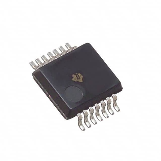
SN74LVC574ADWR Texas Instruments IC FF D-TYPE SNGL 8BIT 20SOIC
Інтэгральныя схемы (ІС)
Нумар вытворцы:
SN74LVC574ADWR
Вытворца:
Катэгорыя прадукцыі:
Апісанне:
IC FF D-TYPE SNGL 8BIT 20SOIC
Стан RoHs:
Табліцы дадзеных:
Бягучы - у стане спакою (Iq) :
1.5µA
Колькасць элементаў :
1
Макс. затрымка распаўсюджвання @ V, макс. CL :
6.8ns @ 3.3V, 50pF
Напружанне - сілкаванне :
1.65 V ~ 3.6 V
Пакет / Чахол :
20-SOIC (0.295", 7.50mm Width)
Працоўная тэмпература :
-40°C ~ 125°C (TA)
серыял :
74LVC
Тактавая частата :
150MHz
Ток - выхад высокі, нізкі :
24mA, 24mA
Тып :
D-Type
Тып вываду :
Tri-State, Non-Inverted
Тып мацавання :
Surface Mount
Тып трыгера :
Positive Edge
Уваходная ёмістасць :
4pF
Ўпакоўка :
Tape & Reel (TR)
Функцыя :
Standard
Частка Статус :
Active
Колькасць біт на элемент :
8
в наличии
22,995
Unit Price:
Звяжыцеся з намі Прапанова
SN74LVC574ADWR Канкурэнтныя кошты
ChipIc мае унікальную крыніцу паставак. Мы можам прапанаваць SN74LVC574ADWR больш
канкурэнтаздольную цану для нашых кліентаў. Вы можаце атрымаць асалоду ад нашым лепшым
сэрвісам, купіўшы ChipIc SN74LVC574ADWR. Калі ласка, не саромейцеся звяртацца наконт
лепшай цаны на SN74LVC574ADWR. Націсніце, каб атрымаць прапанову
SN74LVC574ADWR Асаблівасці
SN74LVC574ADWR is produced by Texas Instruments, belongs to Логіка - Flip Flops.
SN74LVC574ADWR Падрабязная інфармацыя аб прадукцыі
:
SN74LVC574ADWR - гэта Логіка - Flip Flops, буферныя ўзмацняльнікі, распрацаваныя і
вырабленыя
Texas Instruments.
SN74LVC574ADWR вытворчасці Texas Instruments можна набыць на сайце Chipic.
Тут вы можаце знайсці розныя віды электронных дэталяў ад вядучых вытворцаў свету.
SN74LVC574ADWR кампаніі Chipic прайшоў строгі кантроль якасці і адпавядае усім патрабаванням.
Статус запасаў, пазначаны на Chipic, прызначаны толькі для даведкі.
Калі вы не знайшлі запчастку, якую шукаеце, вы можаце звязацца з намі для атрымання дадатковай інфармацыі, такі як колькасць запасаў у табліцы дадзеных SN74LVC574ADWR (PDF), кошт SN74LVC574ADWR, Распіноўка SN74LVC574ADWR, кіраўніцтва SN74LVC574ADWR і рашэнне на замену SN74LVC574ADWR.
SN74LVC574ADWR FAQ
:
1. What is the operating voltage range for the SN74LVC574ADWR?
The operating voltage range for the SN74LVC574ADWR is 2 V to 3.6 V.
2. What is the maximum input clamp current for this device?
The maximum input clamp current for the SN74LVC574ADWR is ±20 mA.
3. Can this device be used in a daisy-chain configuration?
Yes, the SN74LVC574ADWR can be used in a daisy-chain configuration for serial data transfer.
4. What is the typical output rise/fall time for this latch?
The typical output rise/fall time for the SN74LVC574ADWR is 0.8 ns.
5. Is the SN74LVC574ADWR compatible with 5V TTL/CMOS logic levels?
Yes, this device is compatible with 5V TTL/CMOS logic levels when used with appropriate level-shifting techniques.
6. What is the maximum propagation delay for the SN74LVC574ADWR?
The maximum propagation delay for this latch is 5.3 ns.
7. Can the SN74LVC574ADWR withstand electrostatic discharge (ESD)?
Yes, this device has ESD protection and can withstand up to 2000 V human-body model (HBM) ESD.
8. What is the maximum quiescent current consumption of the SN74LVC574ADWR?
The maximum quiescent current consumption of this latch is 10 µA at 25°C.
9. Does the SN74LVC574ADWR have an integrated output diode for inductive load protection?
No, this device does not have an integrated output diode for inductive load protection.
10. What is the package type and dimensions for the SN74LVC574ADWR?
The SN74LVC574ADWR is available in a SOIC-20 package with dimensions of 12.8 mm x 7.5 mm.
SN74LVC574ADWR Змяненні, ключавыя словы
:
SN74LVC574ADWR Кошт
SN74LVC574ADWR Малюнак
SN74LVC574ADWR Напружанне на выснове
Акцыі: Хуткая праверка каціровак
Мінімальная замова: 1
Змяшчае прадукты серыі "SN74"