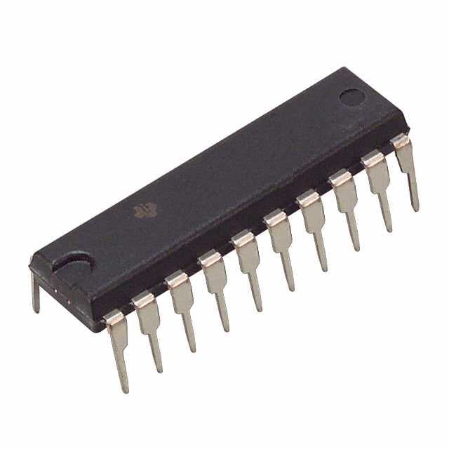
SN74AS832BN Texas Instruments IC GATE OR 6CH 2-INP 20-DIP
Інтэгральныя схемы (ІС)
Нумар вытворцы:
SN74AS832BN
Вытворца:
Катэгорыя прадукцыі:
Апісанне:
IC GATE OR 6CH 2-INP 20-DIP
Стан RoHs:
Табліцы дадзеных:
Асаблівасці :
-
Бягучы - у рэжыме спакою (макс.) :
17mA
Колькасць контураў :
6
Колькасць уваходаў :
2
Лагічны тып :
OR Gate
Макс. затрымка распаўсюджвання @ V, макс. CL :
6.3ns @ 5V, 50pF
Напружанне - сілкаванне :
4.5 V ~ 5.5 V
Пакет / Чахол :
20-DIP (0.300", 7.62mm)
Пакет прылады пастаўшчыка :
20-PDIP
Працоўная тэмпература :
0°C ~ 70°C
серыял :
74AS
Ток - выхад высокі, нізкі :
48mA, 48mA
Тып мацавання :
Through Hole
Узровень логікі - высокі :
2V
Узровень логікі - нізкі :
0.8V
Ўпакоўка :
Tube
Частка Статус :
Active
в наличии
30,284
Unit Price:
Звяжыцеся з намі Прапанова
SN74AS832BN Канкурэнтныя кошты
ChipIc мае унікальную крыніцу паставак. Мы можам прапанаваць SN74AS832BN больш
канкурэнтаздольную цану для нашых кліентаў. Вы можаце атрымаць асалоду ад нашым лепшым
сэрвісам, купіўшы ChipIc SN74AS832BN. Калі ласка, не саромейцеся звяртацца наконт
лепшай цаны на SN74AS832BN. Націсніце, каб атрымаць прапанову
SN74AS832BN Асаблівасці
SN74AS832BN is produced by Texas Instruments, belongs to Логіка - вароты і інвертары.
SN74AS832BN Падрабязная інфармацыя аб прадукцыі
:
SN74AS832BN - гэта Логіка - вароты і інвертары, буферныя ўзмацняльнікі, распрацаваныя і
вырабленыя
Texas Instruments.
SN74AS832BN вытворчасці Texas Instruments можна набыць на сайце Chipic.
Тут вы можаце знайсці розныя віды электронных дэталяў ад вядучых вытворцаў свету.
SN74AS832BN кампаніі Chipic прайшоў строгі кантроль якасці і адпавядае усім патрабаванням.
Статус запасаў, пазначаны на Chipic, прызначаны толькі для даведкі.
Калі вы не знайшлі запчастку, якую шукаеце, вы можаце звязацца з намі для атрымання дадатковай інфармацыі, такі як колькасць запасаў у табліцы дадзеных SN74AS832BN (PDF), кошт SN74AS832BN, Распіноўка SN74AS832BN, кіраўніцтва SN74AS832BN і рашэнне на замену SN74AS832BN.
SN74AS832BN FAQ
:
1. What is the maximum operating frequency of the SN74AS832BN?
The maximum operating frequency of the SN74AS832BN is 100 megahertz.
2. What is the input voltage range for the SN74AS832BN?
The input voltage range for the SN74AS832BN is 4.5V to 5.5V.
3. What is the typical propagation delay of the SN74AS832BN?
The typical propagation delay of the SN74AS832BN is 6 nanoseconds.
4. What is the power dissipation of the SN74AS832BN at maximum frequency?
The power dissipation of the SN74AS832BN at maximum frequency is 550 milliwatts.
5. What is the operating temperature range of the SN74AS832BN?
The operating temperature range of the SN74AS832BN is -40°C to 85°C.
6. What is the package type of the SN74AS832BN?
The package type of the SN74AS832BN is PDIP-16.
7. What is the output drive capability of the SN74AS832BN?
The output drive capability of the SN74AS832BN is ±24 milliamps.
8. Is the SN74AS832BN RoHS compliant?
Yes, the SN74AS832BN is RoHS compliant.
9. What is the pin configuration of the SN74AS832BN?
The pin configuration of the SN74AS832BN is as follows: [Insert pin configuration here]
10. What are the typical applications for the SN74AS832BN?
The typical applications for the SN74AS832BN include memory address decoding and data routing in microprocessor systems.
SN74AS832BN Змяненні, ключавыя словы
:
SN74AS832BN Кошт
SN74AS832BN Малюнак
SN74AS832BN Напружанне на выснове
Акцыі: Хуткая праверка каціровак
Мінімальная замова: 1
Змяшчае прадукты серыі "SN74"