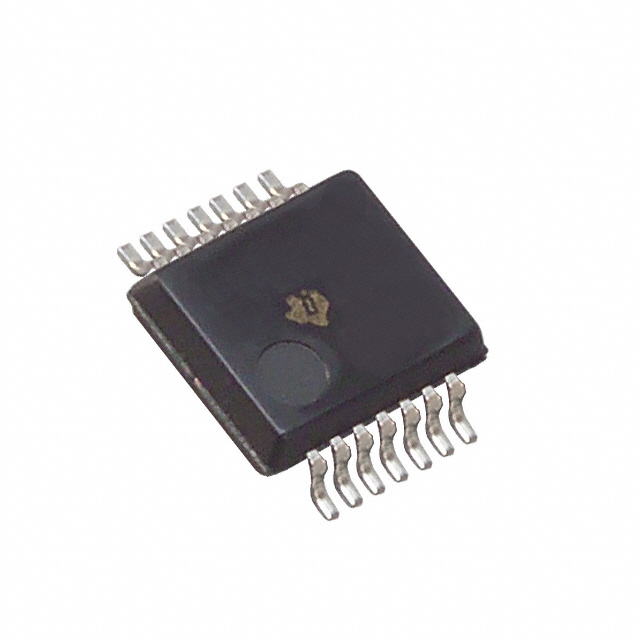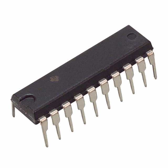
SN74ABT541BN Texas Instruments IC BUF NON-INVERT 5.5V 20PDIP
Інтэгральныя схемы (ІС)
Нумар вытворцы:
SN74ABT541BN
Вытворца:
Катэгорыя прадукцыі:
Апісанне:
IC BUF NON-INVERT 5.5V 20PDIP
Стан RoHs:
Табліцы дадзеных:
Колькасць элементаў :
1
Лагічны тып :
Buffer, Non-Inverting
Напружанне - сілкаванне :
4.5 V ~ 5.5 V
Пакет / Чахол :
20-DIP (0.300", 7.62mm)
Пакет прылады пастаўшчыка :
20-PDIP
Працоўная тэмпература :
-40°C ~ 85°C (TA)
серыял :
74ABT
Ток - выхад высокі, нізкі :
32mA, 64mA
Тып вываду :
Push-Pull
Тып мацавання :
Through Hole
Тып уводу :
-
Ўпакоўка :
Tube
Частка Статус :
Active
Колькасць біт на элемент :
8
в наличии
20,740
Unit Price:
Звяжыцеся з намі Прапанова
SN74ABT541BN Канкурэнтныя кошты
ChipIc мае унікальную крыніцу паставак. Мы можам прапанаваць SN74ABT541BN больш
канкурэнтаздольную цану для нашых кліентаў. Вы можаце атрымаць асалоду ад нашым лепшым
сэрвісам, купіўшы ChipIc SN74ABT541BN. Калі ласка, не саромейцеся звяртацца наконт
лепшай цаны на SN74ABT541BN. Націсніце, каб атрымаць прапанову
SN74ABT541BN Асаблівасці
SN74ABT541BN is produced by Texas Instruments, belongs to Логіка - Буферы, драйверы, прымачы, трансіверы.
SN74ABT541BN Падрабязная інфармацыя аб прадукцыі
:
SN74ABT541BN - гэта Логіка - Буферы, драйверы, прымачы, трансіверы, буферныя ўзмацняльнікі, распрацаваныя і
вырабленыя
Texas Instruments.
SN74ABT541BN вытворчасці Texas Instruments можна набыць на сайце Chipic.
Тут вы можаце знайсці розныя віды электронных дэталяў ад вядучых вытворцаў свету.
SN74ABT541BN кампаніі Chipic прайшоў строгі кантроль якасці і адпавядае усім патрабаванням.
Статус запасаў, пазначаны на Chipic, прызначаны толькі для даведкі.
Калі вы не знайшлі запчастку, якую шукаеце, вы можаце звязацца з намі для атрымання дадатковай інфармацыі, такі як колькасць запасаў у табліцы дадзеных SN74ABT541BN (PDF), кошт SN74ABT541BN, Распіноўка SN74ABT541BN, кіраўніцтва SN74ABT541BN і рашэнне на замену SN74ABT541BN.
SN74ABT541BN FAQ
:
1. What is the maximum operating voltage for the SN74ABT541BN?
The maximum operating voltage for the SN74ABT541BN is 5.5V.
2. What is the typical input high-level voltage for this semiconductor?
The typical input high-level voltage for the SN74ABT541BN is 2V.
3. Can you provide the maximum propagation delay time for this device?
The maximum propagation delay time for the SN74ABT541BN is 6.5ns.
4. What is the output drive capability of the SN74ABT541BN?
The output drive capability of the SN74ABT541BN is ±32mA.
5. Is the SN74ABT541BN compatible with both CMOS and TTL input levels?
Yes, the SN74ABT541BN is compatible with both CMOS and TTL input levels.
6. What is the operating temperature range for this semiconductor?
The operating temperature range for the SN74ABT541BN is -40°C to 85°C.
7. Can you explain the pinout configuration of the SN74ABT541BN?
The SN74ABT541BN has a 20-pin configuration with specific pins designated for input, output, and control functions.
8. Does the SN74ABT541BN have built-in ESD protection?
Yes, the SN74ABT541BN features built-in ESD protection on all pins.
9. What is the typical quiescent current consumption of this device?
The typical quiescent current consumption of the SN74ABT541BN is 80μA.
10. Can you provide information about the package type and dimensions for the SN74ABT541BN?
The SN74ABT541BN is available in a 20-pin TSSOP package with dimensions of 6.50mm x 4.40mm.
SN74ABT541BN Змяненні, ключавыя словы
:
SN74ABT541BN Кошт
SN74ABT541BN Малюнак
SN74ABT541BN Напружанне на выснове
Акцыі: Хуткая праверка каціровак
Мінімальная замова: 1
Змяшчае прадукты серыі "SN74"