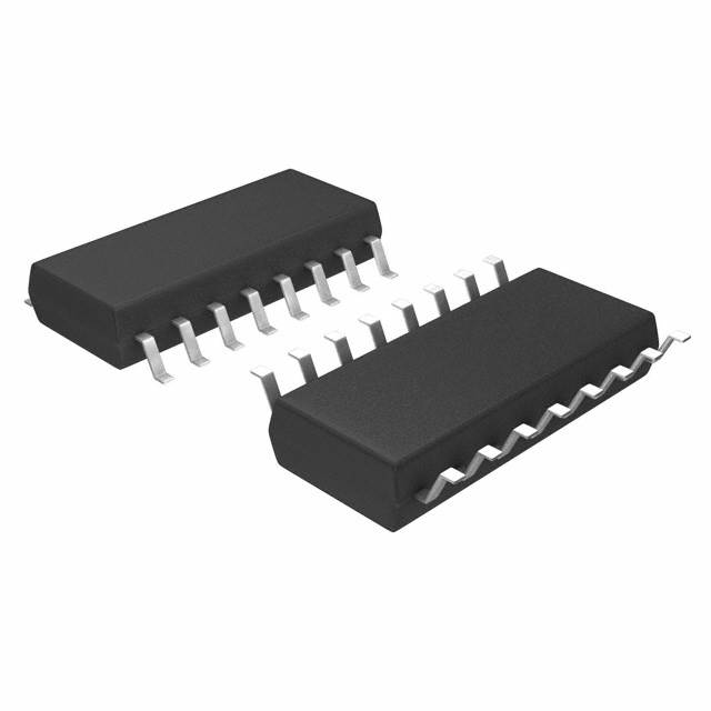
CD4512BNSR Texas Instruments IC DATA SELECTOR 8CH 3ST 16SO
Інтэгральныя схемы (ІС)
Нумар вытворцы:
CD4512BNSR
Вытворца:
Катэгорыя прадукцыі:
Апісанне:
IC DATA SELECTOR 8CH 3ST 16SO
Стан RoHs:
Табліцы дадзеных:
Напружанне - сілкаванне :
3 V ~ 18 V
Незалежныя схемы :
1
Пакет / Чахол :
16-SOIC (0.209", 5.30mm Width)
Пакет прылады пастаўшчыка :
16-SO
Працоўная тэмпература :
-55°C ~ 125°C
серыял :
4000B
Схема :
1 x 8:1
Ток - выхад высокі, нізкі :
6.8mA, 6.8mA
Тып :
Data or/Multiplexer
Тып мацавання :
Surface Mount
Ўпакоўка :
Tape & Reel (TR)
Частка Статус :
Active
Крыніца сілкавання :
Dual Supply
в наличии
51,561
Unit Price:
Звяжыцеся з намі Прапанова
CD4512BNSR Канкурэнтныя кошты
ChipIc мае унікальную крыніцу паставак. Мы можам прапанаваць CD4512BNSR больш
канкурэнтаздольную цану для нашых кліентаў. Вы можаце атрымаць асалоду ад нашым лепшым
сэрвісам, купіўшы ChipIc CD4512BNSR. Калі ласка, не саромейцеся звяртацца наконт
лепшай цаны на CD4512BNSR. Націсніце, каб атрымаць прапанову
CD4512BNSR Асаблівасці
CD4512BNSR is produced by Texas Instruments, belongs to Logic - Сігнальныя камутатары, мультыплексары, дэкодэры.
CD4512BNSR Падрабязная інфармацыя аб прадукцыі
:
CD4512BNSR - гэта Logic - Сігнальныя камутатары, мультыплексары, дэкодэры, буферныя ўзмацняльнікі, распрацаваныя і
вырабленыя
Texas Instruments.
CD4512BNSR вытворчасці Texas Instruments можна набыць на сайце Chipic.
Тут вы можаце знайсці розныя віды электронных дэталяў ад вядучых вытворцаў свету.
CD4512BNSR кампаніі Chipic прайшоў строгі кантроль якасці і адпавядае усім патрабаванням.
Статус запасаў, пазначаны на Chipic, прызначаны толькі для даведкі.
Калі вы не знайшлі запчастку, якую шукаеце, вы можаце звязацца з намі для атрымання дадатковай інфармацыі, такі як колькасць запасаў у табліцы дадзеных CD4512BNSR (PDF), кошт CD4512BNSR, Распіноўка CD4512BNSR, кіраўніцтва CD4512BNSR і рашэнне на замену CD4512BNSR.
CD4512BNSR FAQ
:
1. What is the operating voltage range for CD4512BNSR?
The operating voltage range for CD4512BNSR is 3V to 18V.
2. Can CD4512BNSR be used in automotive applications?
Yes, CD4512BNSR can be used in automotive applications as it is designed to operate within the specified temperature and voltage ranges.
3. What is the maximum output current of CD4512BNSR?
The maximum output current of CD4512BNSR is typically 5.2mA.
4. Is CD4512BNSR a latching device?
No, CD4512BNSR is not a latching device. It is a 8-to-1 line data selector/multiplexer with address latches.
5. What is the typical propagation delay for CD4512BNSR?
The typical propagation delay for CD4512BNSR is 60ns.
6. Can CD4512BNSR tolerate electrostatic discharge (ESD)?
Yes, CD4512BNSR is designed to withstand typical ESD events.
7. What is the package type for CD4512BNSR?
CD4512BNSR is available in a 16-pin SOIC (Shrink Small Outline Package) package.
8. Does CD4512BNSR have built-in input clamping diodes?
Yes, CD4512BNSR has built-in input clamping diodes for overvoltage protection.
9. What is the recommended operating temperature range for CD4512BNSR?
The recommended operating temperature range for CD4512BNSR is -55°C to 125°C.
10. Can CD4512BNSR be cascaded to expand the number of inputs?
Yes, CD4512BNSR can be cascaded to expand the number of inputs by connecting the outputs of one device to the inputs of another.
CD4512BNSR Змяненні, ключавыя словы
:
CD4512BNSR Кошт
CD4512BNSR Малюнак
CD4512BNSR Напружанне на выснове
Акцыі: Хуткая праверка каціровак
Мінімальная замова: 1
Змяшчае прадукты серыі "CD45"