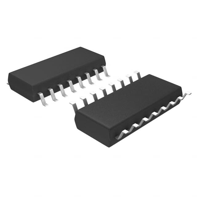
74F399SJ ON Semiconductor IC REGISTER QUAD 2PORT 16SOP
Інтэгральныя схемы (ІС)
Нумар вытворцы:
74F399SJ
Вытворца:
Катэгорыя прадукцыі:
Апісанне:
IC REGISTER QUAD 2PORT 16SOP
Стан RoHs:
Табліцы дадзеных:
Напружанне - сілкаванне :
4.5 V ~ 5.5 V
Незалежныя схемы :
1
Пакет / Чахол :
16-SOIC (0.209", 5.30mm Width)
Пакет прылады пастаўшчыка :
16-SOP
Працоўная тэмпература :
0°C ~ 70°C
серыял :
74F
Схема :
4 x 2:1
Ток - выхад высокі, нізкі :
1mA, 20mA
Тып :
Multiplexer
Тып мацавання :
Surface Mount
Ўпакоўка :
Tube
Частка Статус :
Obsolete
Крыніца сілкавання :
Single Supply
в наличии
35,070
Unit Price:
Звяжыцеся з намі Прапанова
74F399SJ Канкурэнтныя кошты
ChipIc мае унікальную крыніцу паставак. Мы можам прапанаваць 74F399SJ больш
канкурэнтаздольную цану для нашых кліентаў. Вы можаце атрымаць асалоду ад нашым лепшым
сэрвісам, купіўшы ChipIc 74F399SJ. Калі ласка, не саромейцеся звяртацца наконт
лепшай цаны на 74F399SJ. Націсніце, каб атрымаць прапанову
74F399SJ Асаблівасці
74F399SJ is produced by ON Semiconductor, belongs to Logic - Сігнальныя камутатары, мультыплексары, дэкодэры.
74F399SJ Падрабязная інфармацыя аб прадукцыі
:
74F399SJ - гэта Logic - Сігнальныя камутатары, мультыплексары, дэкодэры, буферныя ўзмацняльнікі, распрацаваныя і
вырабленыя
ON Semiconductor.
74F399SJ вытворчасці ON Semiconductor можна набыць на сайце Chipic.
Тут вы можаце знайсці розныя віды электронных дэталяў ад вядучых вытворцаў свету.
74F399SJ кампаніі Chipic прайшоў строгі кантроль якасці і адпавядае усім патрабаванням.
Статус запасаў, пазначаны на Chipic, прызначаны толькі для даведкі.
Калі вы не знайшлі запчастку, якую шукаеце, вы можаце звязацца з намі для атрымання дадатковай інфармацыі, такі як колькасць запасаў у табліцы дадзеных 74F399SJ (PDF), кошт 74F399SJ, Распіноўка 74F399SJ, кіраўніцтва 74F399SJ і рашэнне на замену 74F399SJ.
74F399SJ FAQ
:
1. What is the function of the 74F399SJ semiconductor?
The 74F399SJ is a 8-bit bidirectional universal shift/storage register with 3-state outputs. It can be used for serial-to-parallel or parallel-to-serial data conversion and storage.
2. What is the operating voltage range for the 74F399SJ?
The operating voltage range for the 74F399SJ is typically 4.5V to 5.5V.
3. What is the maximum clock frequency supported by the 74F399SJ?
The 74F399SJ supports a maximum clock frequency of 50MHz.
4. Can the 74F399SJ be cascaded to create a wider shift register?
Yes, the 74F399SJ can be cascaded to create wider shift registers by connecting the serial output of one device to the serial input of the next.
5. What is the typical power consumption of the 74F399SJ?
The typical power consumption of the 74F399SJ is around 40mW.
6. Does the 74F399SJ have built-in output enable functionality?
Yes, the 74F399SJ features a 3-state output enable control for bus-oriented applications.
7. What is the temperature range for operation of the 74F399SJ?
The 74F399SJ is designed to operate within a temperature range of -40°C to 85°C.
8. Can the 74F399SJ tolerate electrostatic discharge (ESD)?
Yes, the 74F399SJ is designed to withstand electrostatic discharge in accordance with industry standards.
9. What package types are available for the 74F399SJ?
The 74F399SJ is available in 16-pin SOIC and 16-pin TSSOP package options.
10. Is there a recommended layout for PCB design when using the 74F399SJ?
Yes, it is recommended to follow the guidelines provided in the datasheet for proper PCB layout and signal integrity considerations when using the 74F399SJ.
74F399SJ Змяненні, ключавыя словы
:
74F399SJ Кошт
74F399SJ Малюнак
74F399SJ Напружанне на выснове
Акцыі: Хуткая праверка каціровак
Мінімальная замова: 1
Змяшчае прадукты серыі "74F3"