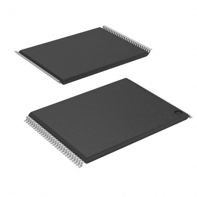
JS28F512M29EWH0 Micron Technology Inc. IC FLASH 512MBIT 110NS 56TSOP
Інтэгральныя схемы (ІС)
Нумар вытворцы:
JS28F512M29EWH0
Вытворца:
Катэгорыя прадукцыі:
Апісанне:
IC FLASH 512MBIT 110NS 56TSOP
Стан RoHs:
Табліцы дадзеных:
Інтэрфейс памяці :
Parallel
Напружанне - сілкаванне :
2.7 V ~ 3.6 V
Пакет / Чахол :
56-TFSOP (0.724", 18.40mm Width)
Пакет прылады пастаўшчыка :
56-TSOP (14x20)
Памер памяці :
512Mb (64M x 8, 32M x 16)
Працоўная тэмпература :
-40°C ~ 85°C (TA)
серыял :
-
Тактавая частата :
-
Тып мацавання :
Surface Mount
Тып памяці :
Non-Volatile
Тэхналогія :
FLASH - NOR
Ўпакоўка :
Tray
Фармат памяці :
Flash
Час доступу :
110ns
Час цыкла запісу - слова, старонка :
110ns
Частка Статус :
Discontinued at Digi-Key
в наличии
42,774
Unit Price:
Звяжыцеся з намі Прапанова
JS28F512M29EWH0 Канкурэнтныя кошты
ChipIc мае унікальную крыніцу паставак. Мы можам прапанаваць JS28F512M29EWH0 больш
канкурэнтаздольную цану для нашых кліентаў. Вы можаце атрымаць асалоду ад нашым лепшым
сэрвісам, купіўшы ChipIc JS28F512M29EWH0. Калі ласка, не саромейцеся звяртацца наконт
лепшай цаны на JS28F512M29EWH0. Націсніце, каб атрымаць прапанову
JS28F512M29EWH0 Асаблівасці
JS28F512M29EWH0 is produced by Micron Technology Inc., belongs to аб'ём памяці.
JS28F512M29EWH0 Падрабязная інфармацыя аб прадукцыі
:
JS28F512M29EWH0 - гэта аб'ём памяці, буферныя ўзмацняльнікі, распрацаваныя і
вырабленыя
Micron Technology Inc..
JS28F512M29EWH0 вытворчасці Micron Technology Inc. можна набыць на сайце Chipic.
Тут вы можаце знайсці розныя віды электронных дэталяў ад вядучых вытворцаў свету.
JS28F512M29EWH0 кампаніі Chipic прайшоў строгі кантроль якасці і адпавядае усім патрабаванням.
Статус запасаў, пазначаны на Chipic, прызначаны толькі для даведкі.
Калі вы не знайшлі запчастку, якую шукаеце, вы можаце звязацца з намі для атрымання дадатковай інфармацыі, такі як колькасць запасаў у табліцы дадзеных JS28F512M29EWH0 (PDF), кошт JS28F512M29EWH0, Распіноўка JS28F512M29EWH0, кіраўніцтва JS28F512M29EWH0 і рашэнне на замену JS28F512M29EWH0.
JS28F512M29EWH0 FAQ
:
1. What is the maximum operating frequency of the JS28F512M29EWH0 flash memory?
The maximum operating frequency of the JS28F512M29EWH0 flash memory is 133 MHz.
2. What is the typical power consumption of the JS28F512M29EWH0 during read operations?
The typical power consumption of the JS28F512M29EWH0 during read operations is 60 mA.
3. Can the JS28F512M29EWH0 operate at extended temperature ranges?
Yes, the JS28F512M29EWH0 is designed to operate at extended temperature ranges from -40°C to 85°C.
4. What is the programming voltage range for the JS28F512M29EWH0?
The programming voltage range for the JS28F512M29EWH0 is 2.7V to 3.6V.
5. Does the JS28F512M29EWH0 support hardware data protection features?
Yes, the JS28F512M29EWH0 supports hardware data protection features such as block lock and OTP (one-time programmable) memory.
6. What is the maximum erase cycle endurance of the JS28F512M29EWH0?
The JS28F512M29EWH0 has a maximum erase cycle endurance of 100,000 cycles per block.
7. Is the JS28F512M29EWH0 compatible with standard flash memory interfaces?
Yes, the JS28F512M29EWH0 is compatible with standard flash memory interfaces such as SPI (Serial Peripheral Interface) and I2C (Inter-Integrated Circuit).
8. What is the size of the erase block for the JS28F512M29EWH0?
The erase block size for the JS28F512M29EWH0 is 128 KB.
9. Can the JS28F512M29EWH0 be used in automotive applications?
Yes, the JS28F512M29EWH0 is qualified for automotive applications and meets AEC-Q100 requirements.
10. What are the available package options for the JS28F512M29EWH0?
The JS28F512M29EWH0 is available in industry-standard packages such as TSOP and BGA.
JS28F512M29EWH0 Змяненні, ключавыя словы
:
JS28F512M29EWH0 Кошт
JS28F512M29EWH0 Малюнак
JS28F512M29EWH0 Напружанне на выснове
Акцыі: Хуткая праверка каціровак
Мінімальная замова: 1
Змяшчае прадукты серыі "JS28"