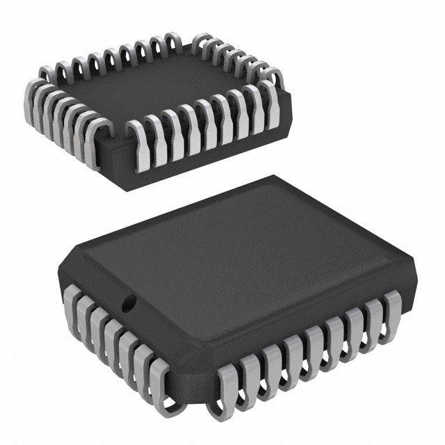
AT49BV001ANT-55VI Microchip Technology IC FLASH 1MBIT 55NS 32VSOP
Інтэгральныя схемы (ІС)
Нумар вытворцы:
AT49BV001ANT-55VI
Вытворца:
Катэгорыя прадукцыі:
Апісанне:
IC FLASH 1MBIT 55NS 32VSOP
Стан RoHs:
Табліцы дадзеных:
Інтэрфейс памяці :
Parallel
Напружанне - сілкаванне :
2.7 V ~ 3.6 V
Пакет / Чахол :
32-TFSOP (0.488", 12.40mm Width)
Пакет прылады пастаўшчыка :
32-VSOP
Памер памяці :
1Mb (128K x 8)
Працоўная тэмпература :
-40°C ~ 85°C (TC)
серыял :
-
Тактавая частата :
-
Тып мацавання :
Surface Mount
Тып памяці :
Non-Volatile
Тэхналогія :
Flash
Ўпакоўка :
Tray
Фармат памяці :
Flash
Час доступу :
55ns
Час цыкла запісу - слова, старонка :
50µs
Частка Статус :
Obsolete
в наличии
59,321
Unit Price:
Звяжыцеся з намі Прапанова
AT49BV001ANT-55VI Канкурэнтныя кошты
ChipIc мае унікальную крыніцу паставак. Мы можам прапанаваць AT49BV001ANT-55VI больш
канкурэнтаздольную цану для нашых кліентаў. Вы можаце атрымаць асалоду ад нашым лепшым
сэрвісам, купіўшы ChipIc AT49BV001ANT-55VI. Калі ласка, не саромейцеся звяртацца наконт
лепшай цаны на AT49BV001ANT-55VI. Націсніце, каб атрымаць прапанову
AT49BV001ANT-55VI Асаблівасці
AT49BV001ANT-55VI is produced by Microchip Technology, belongs to аб'ём памяці.
AT49BV001ANT-55VI Падрабязная інфармацыя аб прадукцыі
:
AT49BV001ANT-55VI - гэта аб'ём памяці, буферныя ўзмацняльнікі, распрацаваныя і
вырабленыя
Microchip Technology.
AT49BV001ANT-55VI вытворчасці Microchip Technology можна набыць на сайце Chipic.
Тут вы можаце знайсці розныя віды электронных дэталяў ад вядучых вытворцаў свету.
AT49BV001ANT-55VI кампаніі Chipic прайшоў строгі кантроль якасці і адпавядае усім патрабаванням.
Статус запасаў, пазначаны на Chipic, прызначаны толькі для даведкі.
Калі вы не знайшлі запчастку, якую шукаеце, вы можаце звязацца з намі для атрымання дадатковай інфармацыі, такі як колькасць запасаў у табліцы дадзеных AT49BV001ANT-55VI (PDF), кошт AT49BV001ANT-55VI, Распіноўка AT49BV001ANT-55VI, кіраўніцтва AT49BV001ANT-55VI і рашэнне на замену AT49BV001ANT-55VI.
AT49BV001ANT-55VI FAQ
:
1. What is the maximum operating frequency of the AT49BV001ANT-55VI flash memory?
The maximum operating frequency of the AT49BV001ANT-55VI flash memory is 55 MHz.
2. What is the voltage range for the input and output buffers of the AT49BV001ANT-55VI?
The voltage range for the input and output buffers of the AT49BV001ANT-55VI is 2.7V to 3.6V.
3. Can the AT49BV001ANT-55VI operate in both synchronous and asynchronous modes?
Yes, the AT49BV001ANT-55VI can operate in both synchronous and asynchronous modes.
4. What is the typical access time of the AT49BV001ANT-55VI flash memory?
The typical access time of the AT49BV001ANT-55VI flash memory is 55ns.
5. Does the AT49BV001ANT-55VI support sector erase and chip erase operations?
Yes, the AT49BV001ANT-55VI supports both sector erase and chip erase operations.
6. What is the maximum data retention period of the AT49BV001ANT-55VI?
The maximum data retention period of the AT49BV001ANT-55VI is 20 years.
7. Is the AT49BV001ANT-55VI compatible with both 5V and 3.3V systems?
Yes, the AT49BV001ANT-55VI is compatible with both 5V and 3.3V systems.
8. What is the temperature range for the operation of the AT49BV001ANT-55VI?
The temperature range for the operation of the AT49BV001ANT-55VI is -40°C to 85°C.
9. Can the AT49BV001ANT-55VI be used for in-system programming (ISP)?
Yes, the AT49BV001ANT-55VI can be used for in-system programming (ISP).
10. What is the package type of the AT49BV001ANT-55VI flash memory?
The AT49BV001ANT-55VI flash memory is available in a 32-lead PLCC package.
AT49BV001ANT-55VI Змяненні, ключавыя словы
:
AT49BV001ANT-55VI Кошт
AT49BV001ANT-55VI Малюнак
AT49BV001ANT-55VI Напружанне на выснове
Акцыі: Хуткая праверка каціровак
Мінімальная замова: 1
Змяшчае прадукты серыі "AT49"