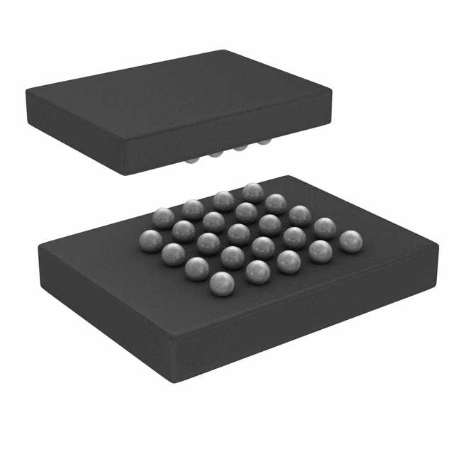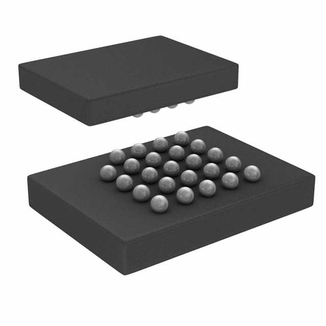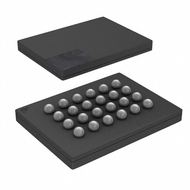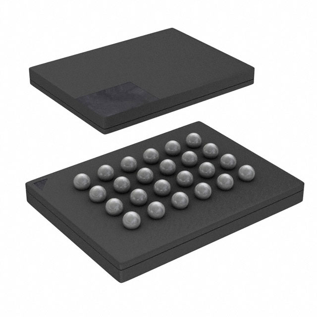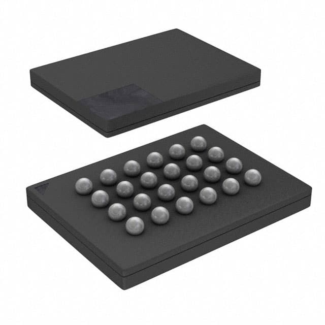
S25FL064P0XNFV001M Cypress Semiconductor Corp IC FLASH NOR
Інтэгральныя схемы (ІС)
Нумар вытворцы:
S25FL064P0XNFV001M
Вытворца:
Катэгорыя прадукцыі:
Апісанне:
IC FLASH NOR
Стан RoHs:
 Без свінцу / у адпаведнасці з RoHS
 Табліцы дадзеных:

Інтэрфейс памяці :
SPI - Quad I/O
Напружанне - сілкаванне :
2.7 V ~ 3.6 V
Пакет / Чахол :
-
Пакет прылады пастаўшчыка :
-
Памер памяці :
64Mb (8M x 8)
Працоўная тэмпература :
-40°C ~ 105°C (TA)
серыял :
FL-P
Тактавая частата :
104MHz
Тып мацавання :
-
Тып памяці :
Non-Volatile
Тэхналогія :
FLASH - NOR
Ўпакоўка :
-
Фармат памяці :
Flash
Час доступу :
-
Час цыкла запісу - слова, старонка :
5µs, 3ms
Частка Статус :
Obsolete
в наличии
11,994
Unit Price:
Звяжыцеся з намі Прапанова
S25FL064P0XNFV001M Канкурэнтныя кошты
ChipIc мае унікальную крыніцу паставак. Мы можам прапанаваць S25FL064P0XNFV001M больш
канкурэнтаздольную цану для нашых кліентаў. Вы можаце атрымаць асалоду ад нашым лепшым
сэрвісам, купіўшы ChipIc S25FL064P0XNFV001M. Калі ласка, не саромейцеся звяртацца наконт
лепшай цаны на S25FL064P0XNFV001M. Націсніце, каб атрымаць прапанову
S25FL064P0XNFV001M Асаблівасці
S25FL064P0XNFV001M is produced by Cypress Semiconductor Corp, belongs to аб'ём памяці.
S25FL064P0XNFV001M Падрабязная інфармацыя аб прадукцыі
:
S25FL064P0XNFV001M - гэта аб'ём памяці, буферныя ўзмацняльнікі, распрацаваныя і
вырабленыя
Cypress Semiconductor Corp.
S25FL064P0XNFV001M вытворчасці Cypress Semiconductor Corp можна набыць на сайце Chipic.
Тут вы можаце знайсці розныя віды электронных дэталяў ад вядучых вытворцаў свету.
S25FL064P0XNFV001M кампаніі Chipic прайшоў строгі кантроль якасці і адпавядае усім патрабаванням.
Статус запасаў, пазначаны на Chipic, прызначаны толькі для даведкі.
Калі вы не знайшлі запчастку, якую шукаеце, вы можаце звязацца з намі для атрымання дадатковай інфармацыі, такі як колькасць запасаў у табліцы дадзеных S25FL064P0XNFV001M (PDF), кошт S25FL064P0XNFV001M, Распіноўка S25FL064P0XNFV001M, кіраўніцтва S25FL064P0XNFV001M і рашэнне на замену S25FL064P0XNFV001M.
S25FL064P0XNFV001M вытворчасці Cypress Semiconductor Corp можна набыць на сайце Chipic.
Тут вы можаце знайсці розныя віды электронных дэталяў ад вядучых вытворцаў свету.
S25FL064P0XNFV001M кампаніі Chipic прайшоў строгі кантроль якасці і адпавядае усім патрабаванням.
Статус запасаў, пазначаны на Chipic, прызначаны толькі для даведкі.
Калі вы не знайшлі запчастку, якую шукаеце, вы можаце звязацца з намі для атрымання дадатковай інфармацыі, такі як колькасць запасаў у табліцы дадзеных S25FL064P0XNFV001M (PDF), кошт S25FL064P0XNFV001M, Распіноўка S25FL064P0XNFV001M, кіраўніцтва S25FL064P0XNFV001M і рашэнне на замену S25FL064P0XNFV001M.
S25FL064P0XNFV001M FAQ
:
1. What is the maximum clock frequency of the S25FL064P0XNFV001M?
The maximum clock frequency of the S25FL064P0XNFV001M is 133 MHz.
2. What is the operating voltage range of the S25FL064P0XNFV001M?
The operating voltage range of the S25FL064P0XNFV001M is 2.7V to 3.6V.
3. What is the size of the memory array in the S25FL064P0XNFV001M?
The memory array size of the S25FL064P0XNFV001M is 8,388,608 bytes.
4. Does the S25FL064P0XNFV001M support sector erase operation?
Yes, the S25FL064P0XNFV001M supports sector erase operation.
5. What is the typical power consumption of the S25FL064P0XNFV001M during read operation?
The typical power consumption of the S25FL064P0XNFV001M during read operation is 4 mA.
6. Can the S25FL064P0XNFV001M operate in extended temperature ranges?
Yes, the S25FL064P0XNFV001M can operate in extended temperature ranges from -40°C to 85°C.
7. What is the maximum data transfer rate of the S25FL064P0XNFV001M in Quad SPI mode?
The maximum data transfer rate of the S25FL064P0XNFV001M in Quad SPI mode is 532 Mbps.
8. Does the S25FL064P0XNFV001M support software protection features?
Yes, the S25FL064P0XNFV001M supports software protection features for memory sectors.
9. What is the package type of the S25FL064P0XNFV001M?
The package type of the S25FL064P0XNFV001M is 8-contact WSON (6mm x 8mm).
10. Is the S25FL064P0XNFV001M RoHS compliant?
Yes, the S25FL064P0XNFV001M is RoHS compliant.
The maximum clock frequency of the S25FL064P0XNFV001M is 133 MHz.
2. What is the operating voltage range of the S25FL064P0XNFV001M?
The operating voltage range of the S25FL064P0XNFV001M is 2.7V to 3.6V.
3. What is the size of the memory array in the S25FL064P0XNFV001M?
The memory array size of the S25FL064P0XNFV001M is 8,388,608 bytes.
4. Does the S25FL064P0XNFV001M support sector erase operation?
Yes, the S25FL064P0XNFV001M supports sector erase operation.
5. What is the typical power consumption of the S25FL064P0XNFV001M during read operation?
The typical power consumption of the S25FL064P0XNFV001M during read operation is 4 mA.
6. Can the S25FL064P0XNFV001M operate in extended temperature ranges?
Yes, the S25FL064P0XNFV001M can operate in extended temperature ranges from -40°C to 85°C.
7. What is the maximum data transfer rate of the S25FL064P0XNFV001M in Quad SPI mode?
The maximum data transfer rate of the S25FL064P0XNFV001M in Quad SPI mode is 532 Mbps.
8. Does the S25FL064P0XNFV001M support software protection features?
Yes, the S25FL064P0XNFV001M supports software protection features for memory sectors.
9. What is the package type of the S25FL064P0XNFV001M?
The package type of the S25FL064P0XNFV001M is 8-contact WSON (6mm x 8mm).
10. Is the S25FL064P0XNFV001M RoHS compliant?
Yes, the S25FL064P0XNFV001M is RoHS compliant.
S25FL064P0XNFV001M Змяненні, ключавыя словы
:
S25FL064P0XNFV001M Кошт
S25FL064P0XNFV001M Малюнак
S25FL064P0XNFV001M Напружанне на выснове
Акцыі: Хуткая праверка каціровак
Мінімальная замова: 1
Змяшчае прадукты серыі "S25F"